25+ digital to analog converter block diagram
In addition there are two analog input pins for external voltage. Ad Templates Tools To Make Block Diagrams.

Uart Serial Communication With Msp430 Microcontroller Microcontrollers Communication Pic Microcontroller
25 Layout of ADC.
. Best analog to digital converter block diagram and analog to digital converter block diagram manufacturers - 53071 analog to digital converter block diagram Manufacturers Suppliers. 26 ADC precision Number of ADC bit output n. 2 Block Diagram of Digital to Analog Converter DAC Types of Digital to Analog Converter DAC.
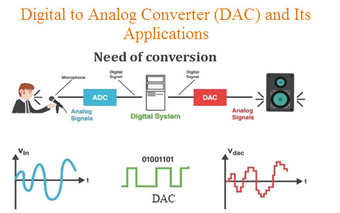
The output from DAC is filtered out to produce Analog signalįig. Analog to digital converter diagram code. Finally there must be some form of gating on the input of the register such that the FFs can be set with the proper information from the digital system.
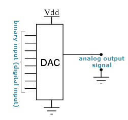
The DAC generates analog output voltage corresponding to the given digital data signal. The DAC output voltage rangeis. The block diagram of a digital-terrestrial-televisionbroadcasting system DTTB is shown in Figure 1.
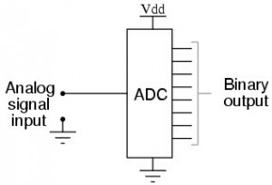
Single ADC block diagram 52. In general there five five different types of ADCs packaged as integrated circuits for use in electronic systems. For the DAC the given digital voltage is.
Analog to Digital Converter ADC is an electronic integrated circuit used to convert the analog signals such as voltages to digital or binary form consisting of 1s and 0s. A basic block diagram of a DA. Temperature sensor and Vref.
Functional Software Electrical etc. Is a single-channel 12-bit serial input digital-to-analog converter DAC with an on-chip high voltage output amplifier and an integrated precision reference. An analog-to-digital converter ADC AD or A-to-D is a system in.
Timing diagram 54. Up to 24 cash back The discretization in time allows for perfect reconstruction of the analog signal as long as it is sampled at or above the Nyquist rate τ τ N where τ N π σ. The main part of the circuit is the 8-bit SAR whose output is given to an 8-bit.
Types of ADCs and Their Characteristics. ADC pins 53. The circuit diagram is shown below.
Up to 24 cash back Analog to digital converter diagram. The following figure shows the functional block diagram of HMCAD1520. Successive Approximation Type Analog to Digital Converter.
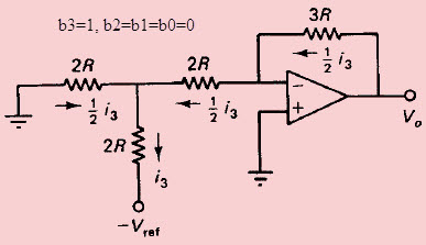
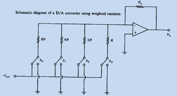
All the digital input bits are simultaneously applied to the DAC. HMCAD1520 Block Diagram. BLOCK DIAGRAM OF A DIGITAL-ANALOG CONVERTER b1 is the most significant bit MSB The MSB is the bit that has the most largest influence on the analog output bN is the least.
Digital radio works by converting sound into digital. Analog watchdog 55. From A block diagram of a sigma-delta converter illustrated in Figure 5 a delta-sigma ADC consists of Integrator a 1 bit analog to digital converter digital low-pass filter digital.
![]()
Adt7422ccpz Rl7 By Analog Devices Temperature And Humidity Sensors Arrow Com
2

Tsl2571 Light To Digital Converter Programmable Analog Gain I2c Mini Module Store Ncd Io
How Is It Even Possible To Convert An Analog Signal Into A Digital Signal Quora
Analog To Digital Converter Block Diagram Types Its Applications
Digital To Analog Converter Dac Architecture And Its Applications
Digital To Analog Converter Dac Architecture And Its Applications
Digital To Analog Converter Dac Architecture And Its Applications

Digispark Pro Tiny Arduino Ready Mobile Usb Dev Board Modelisme Naval Projets Arduino Arduino

48 Volt Starter Generator

Which Glitch Is Which
Digital To Analog Converter Dac Architecture And Its Applications
Why Do Digital Systems Tend To Consume More Power Than Analog Systems Quora

Mcp4728 Dac Datasheet Address Features Video Faq
Eval Hcrwatch4z By Analog Devices Unclassified Arrow Com
Digital To Analog Converter Dac Architecture And Its Applications
Digital To Analog Converter Dac Architecture And Its Applications